SEGGER Evaluation Software for Keil MCB1700
SEGGER Evaluation Software
SEGGER Notifications
Subscribe to SEGGER Evaluation Software Notifications
Data Sheets
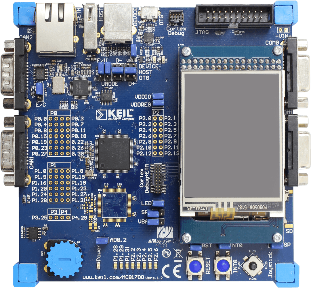
Keil MCB1700
- 100MHz ARM Cortex-M3 processor-based MCU
- On-Chip Memory: 512KB Flash and 64KB RAM
- Color QVGA TFT LCD
- 10/100 Ethernet Port
- USB 2.0 Full Speed - USB, USB-OTG, and USB Host
- 2 CAN interfaces
- 2 Serial Ports
- SD/MMC Card Interface
- 5-position Joystick and push-button
- Analog Voltage Control for ACD Input
- Amplifier and Speaker
- Up to 70 GPIO
- Debug Interface Connectors
- 20-pin JTAG (0.1 inch connector)
- 10-pin Cortex debug (0.05 inch connector)
- 20-pin Cortex debug + ETM Trace (0.05 inch connector)
LPC1768FBD100
- Arm Cortex-M3 processor, running at frequencies of up to 100 MHz
- Arm Cortex-M3 built-in Nested Vectored Interrupt Controller (NVIC)
- 32/16 kB of SRAM on the CPU with local code/data bus for high-performance CPU access
- 32-bit ARM Cortex-M3 microcontroller
- Two/one 16 kB SRAM blocks with separate access paths for higher throughput
- Eight channel General Purpose DMA controller (GPDMA) on the AHB multilayer matrix that can be used with SSP, I2S-bus, UART, Analog-to-Digital and Digital-to-Analog converter peripherals, timer match signals, and for memory-to-memory transfers
- Multilayer AHB matrix interconnect provides a separate bus for each AHB master
- Ethernet MAC with RMII interface and dedicated DMA controller
- USB 2.0 full-speed device/Host/OTG controller with dedicated DMA controller and on-chip PHY for device, Host, and OTG functions
- Four UARTs with fractional baud rate generation, internal FIFO, and DMA support
- One UART has modem control I/O and RS-485/EIA-485 support, and one UART has IrDA support
- CAN 2.0B controller with two channels
- SPI controller with synchronous, serial, full duplex communication and programmable data length
- Two SSP controllers with FIFO and multi-protocol capabilities. The SSP interfaces can be used with the GPDMA controller
- Three enhanced I2C bus interfaces, one with an open-drain output supporting full I2C specification and Fast mode plus with data rates of 1 Mbit/s, two with standard port pins
- I2S (Inter-IC Sound) interface for digital audio input or output, with fractional rate control. The I2S-bus interface can be used with the GPDMA
- 70 (100 pin package) General Purpose I/O (GPIO) pins with configurable pull-up/down resistors
- 12-bit Analog-to-Digital Converter (ADC) with input multiplexing among eight pins, conversion rates up to 200 kHz, and multiple result registers
- 10-bit Digital-to-Analog Converter (DAC) with dedicated conversion timer and DMA support
- One motor control PWM with support for three-phase motor control
- 32-bit ARM Cortex-M3 microcontroller
- Quadrature encoder interface that can monitor one external quadrature encoder
- One standard PWM/timer block with external count input
- RTC with a separate power domain and dedicated RTC oscillator
- WatchDog Timer (WDT). The WDT can be clocked from the internal RC oscillator,
- the RTC oscillator, or the APB clock.
- Arm Cortex-M3 system tick timer, including an external clock input option
- Standard JTAG debug interface for compatibility with existing tools
- Emulation trace module enables non-intrusive, high-speed real-time tracing of instruction execution
- Integrated PMU (Power Management Unit) automatically adjusts internal regulators to minimize power consumption during Sleep, Deep sleep, Power-down, and Deep power-down modes
- Four reduced power modes: Sleep, Deep-sleep, Power-down, and Deep power-down.
- Single 3.3 V power supply (2.4 V to 3.6 V)
- Four external interrupt inputs configurable as edge/level sensitive. All pins on Port 0 and Port 2 can be used as edge sensitive interrupt sources
- Non-maskable Interrupt (NMI) input
- Clock output function that can reflect the main oscillator clock, IRC clock, RTC clock, CPU clock, and the USB clock
- The Wake-up Interrupt Controller (WIC) allows the CPU to automatically wake up from any priority interrupt that can occur while the clocks are stopped in deep sleep, Power-down, and Deep power-down modes
- Brownout detect with separate threshold for interrupt and forced reset
- Power-On Reset (POR)
- Crystal oscillator with an operating range of 1 MHz to 25 MHz
- 4 MHz internal RC oscillator trimmed to 1 % accuracy that can optionally be used as a system clock
- USB PLL for added flexibility
- Code Read Protection (CRP) with different security levels