RX Adapter
Seamless connectivity for J-Link
- Renesas RX100/200/600 support
- FINE interface support
Overview
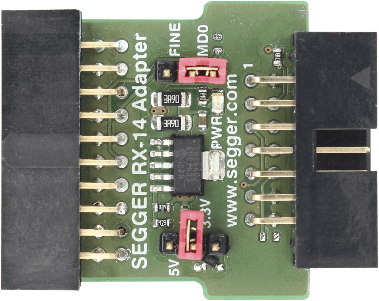
The RX Adapter allows connections between J-Link or Flasher and target hardware which comes with the Renesas RX600 / 200 / 100 series MCUs. When using the RX Adapter, please make sure that you are using the latest revision of this adapter, since on older revisions specific features like FINE interface support may not be supported. The back-side of the adapter shows the revision of it. The current revision is 5. Older revisions may not show a revision on the back-side but a production date only. Please replace these adapters with one of revision 5 or newer.

The RX adapter is able to optionally power the connected target hardware. 3.3 V or 5 V supply voltage can be selected using a Jumper. The target is supplied via the VTref connection (pin 8) when the supply option is jumpered. The RX Adapter is shipped with option "do not power target" (jumper open)
Pinouts and Jumper Settings
FINE Connection
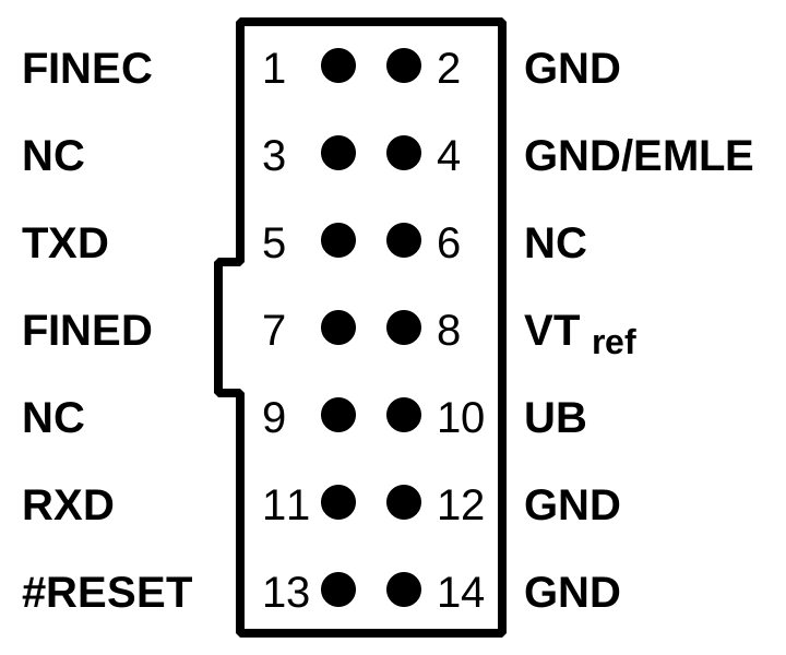
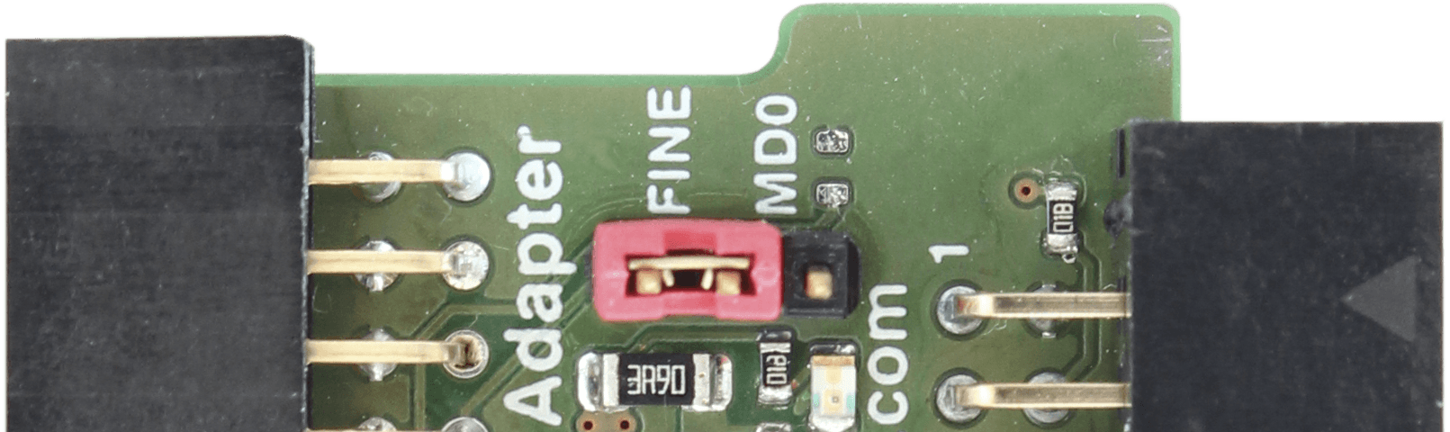
It can also be used for connecting via FINE to the following cores:
- RX111
- RX13T
- RX140
- RX210
- RX21A
- RX220
Please note:
For connecting to RX63x or RX72N devices via FINE, the RX FINE Adapter is required.
JTAG Connection
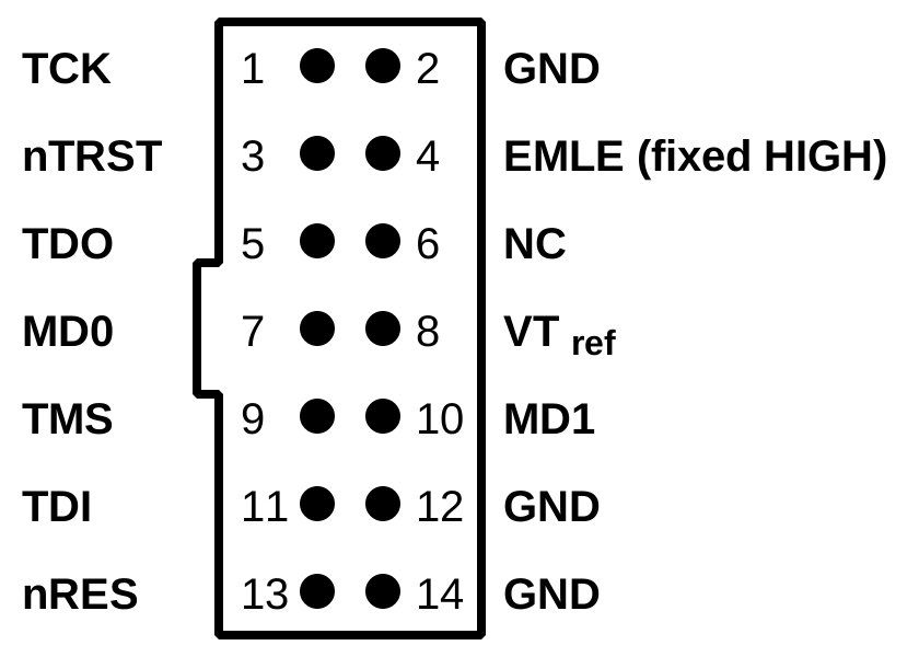
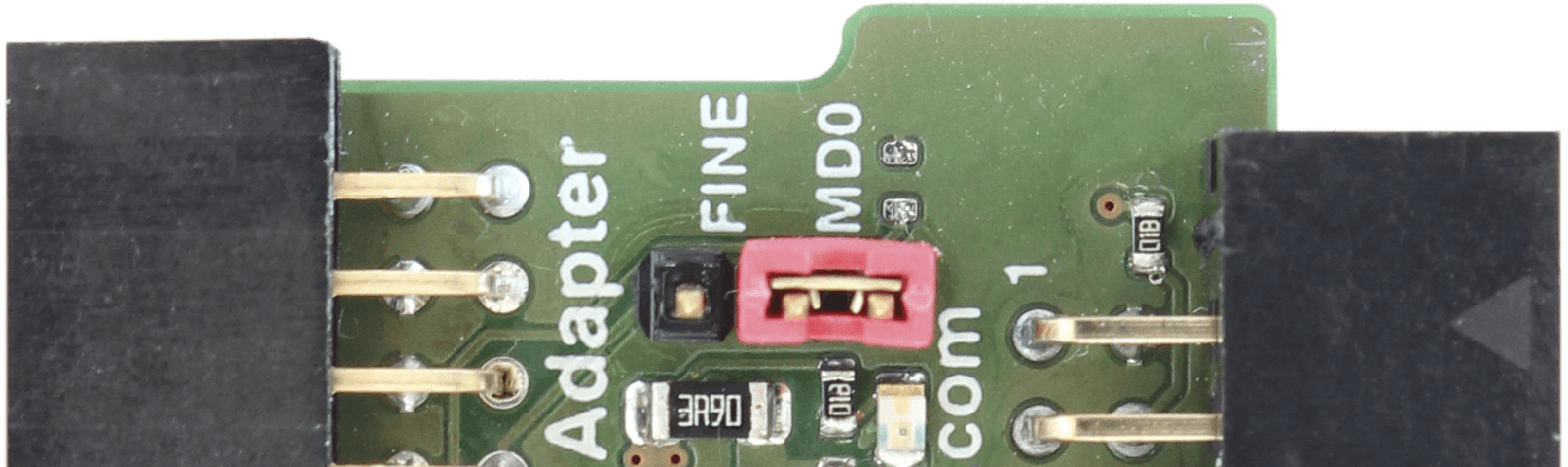
The RX Adapter supports connecting via JTAG to the following cores:
- RX610
- RX621
- RX62G
- RX62N
- RX62T
- RX630
- RX631
- RX63N
- RX63T
- RX64M
- RX65N
- RX660
- RX66T
- RX71M
- RX72N
The FINED Signal: Since the FINE interface is a open-drain specified interface, there is always a pull-up necessary on the target hardware. Pull-up recommendation is 1k Ohm.
CPU Signal <-> RX Adapter Connection
In the following, for the different Renesas RX CPUs the CPU signal <-> J-Link RX Adapter signal mapping is described.
RX111 CPUs:
The following table shows the mapping for FINE. This core does not support JTAG.
- CPU signal / pin name
- RX Adapter pin / signal name
- FINEC / P27
- Pin 1 (FINEC)
- NC
- Pin 4 (EMLE)
- MD_FINED (via pull-up)
- Pin 7 (FINED)
- P14
- Pin 10 (UB)
- RESn
- Pin 13 (nRES)
RX210 CPUs:
The following table shows the mapping for FINE. This core does not support JTAG.
- CPU signal / pin name
- RX Adapter pin / signal name
- SCK1 / P27
- Pin 1 (FINEC)
- NC
- Pin 4 (EMLE)
- MODE / MD_FINED (via pull-up)
- Pin 7 (FINED)
- UB / PC7
- Pin 10 (UB)
- RESET_N / nRES
- Pin 13 (nRES)
RX220 CPUs:
The following table shows the mapping for FINE. This core does not support JTAG.
- CPU signal / pin name
- RX Adapter pin / signal name
- SCK1 / P27
- Pin 1 (FINEC)
- NC
- Pin 4 (EMLE)
- MODE / MD_FINED (via pull-up)
- Pin 7 (FINED)
- UB / PC7
- Pin 10 (UB)
- RESET_N / nRES
- Pin 13 (nRES)
RX630 CPUs:
This core supports FINE and JTAG. The following table shows the mapping for JTAG.
To operate the FINE interface of this core please use the RX FINE Adapter.
- CPU signal / pin name
- RX Adapter pin / signal name
- P27 / TCK / FINEC
- Pin 1 (TCK)
- TRSTn
- Pin 3 (nTRST)
- EMLE
- Pin 4 (EMLE)
- TDO
- Pin 5 (TDO)
- MD_FINED (via pull-up)
- Pin 7 (MD0)
- TMS
- Pin 9 (TMS)
- IRQ14 / PC7
- Pin 10 (UB)
- TDI
- Pin 11 (TDI)
- RESn
- Pin 13 (nRES)
RX631 / RX63N CPUs:
This core supports FINE and JTAG. The following table shows the mapping for JTAG.
To operate the FINE interface of this core please use the RX FINE Adapter.
- CPU signal / pin name
- RX Adapter pin / signal name
- P27 / TCK / FINEC
- Pin 1 (TCK)
- TRSTn
- Pin 3 (nTRST)
- EMLE
- Pin 4 (EMLE)
- TDO
- Pin 5 (TDO)
- MD_FINED (via pull-up)
- Pin 7 (MD0)
- TMS
- Pin 9 (TMS)
- IRQ14 / PC7
- Pin 10 (UB)
- TDI
- Pin 11 (TDI)
- RESn
- Pin 13 (nRES)
RX63T CPUs:
This core supports FINE and JTAG. The following table shows the mapping for JTAG.
To operate the FINE interface of this core please use the RX FINE Adapter.
- CPU signal / pin name
- RX Adapter pin / signal name
- P27 / TCK / FINEC
- Pin 1 (TCK)
- TRSTn
- Pin 3 (nTRST)
- EMLE
- Pin 4 (EMLE)
- TDO
- Pin 5 (TDO)
- MD_FINED (via pull-up)
- Pin 7 (MD0)
- TMS
- Pin 9 (TMS)
- IRQ14 / PC7
- Pin 10 (UB)
- TDI
- Pin 11 (TDI)
- RESn
- Pin 13 (nRES)
RX72N CPUs:
This core supports FINE and JTAG. The following table shows the mapping for JTAG.
To operate the FINE interface of this core please use the RX FINE Adapter.
- CPU signal / pin name
- RX Adapter pin / signal name
- TCK
- Pin 1 (TCK)
- TRSTn
- Pin 3 (nTRST)
- EMLE
- Pin 4 (EMLE)
- TDO
- Pin 5 (TDO)
- MD (via pull-up)
- Pin 7 (MD0)
- TMS
- Pin 9 (TMS)
- UB
- Pin 10 (UB)
- TDI
- Pin 11 (TDI)
- RESn
- Pin 13 (nRES)
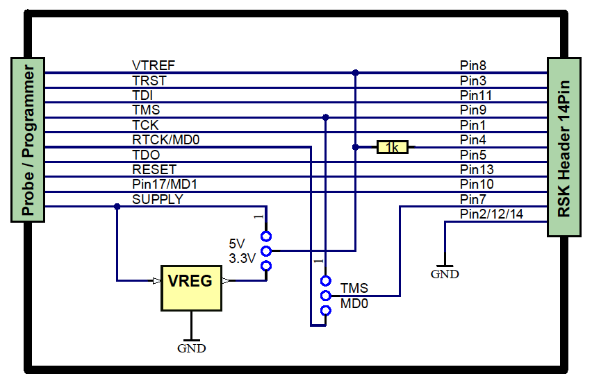
Schematics
The following functional block diagram illustrates the connections between the debug probe and the target.
Get in touch with us
Have questions or need assistance? Our Embedded Experts are here to help!
Reach out to us for:
- Licensing quotes
- Technical inquiries
- Project support