
Overview
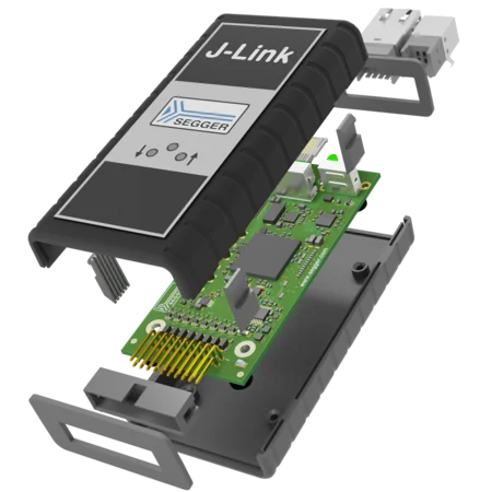
J-Link PLUS is a USB-powered JTAG/SWD debug probe based on a 32-bit RISC CPU. It supports a wide range of CPU cores and offers high-speed communication capabilities. J-Links are widely used for embedded development and production (flash programming) around the world, and they are supported by all major integrated development environments (IDEs), including Eclipse, GDB-based IDEs, and SEGGER Embedded Studio.
A complete list of supported IDEs is available here. Altogether, more than 500,000 J-Links have been shipped, making J-Link the de facto standard debug probe for Arm cores.
Key features

High download speeds
J-Link PLUS offers download speeds of up to 1 MB/s, ensuring that project development moves forward smoothly and reliably, with minimized download times.
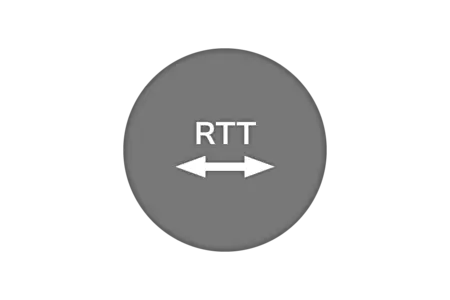
Real Time Transfer
J-Link PLUS offers Real Time Transfer (RTT), which provides a simplified path for information to travel when an application is running. Users can also easily monitor changes in operation.
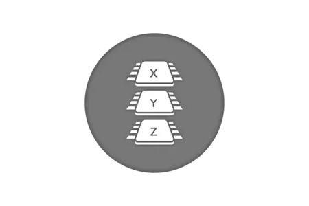
Broad CPU and IDE support
J-Link PLUS works with an extensive range of microcontrollers and IDEs. It enables users to connect their selected microcontroller with their favorite IDE.
Supported devices
The list of supported manufacturers, families, devices, and SoCs includes tens of thousands of devices in hundreds of device families.
Device not listed? Please don’t hesitate to contact us.
Use cases
Communication testing
When testing communication protocols such as Wi-Fi, ZigBee, or Matter, large-scale test setups are crucial for ensuring reliability and performance. A test farm using J-Link PLUS provides a way to test devices under various conditions and ensure that they can handle interference and high traffic volumes.
Integration into rigs
J-Link PLUS Compact's smaller form factor versus other J-Link devices makes it an ideal choice for integration into automated rigs and production environments. Its small size, combined with powerful functionality, allows it to be seamlessly incorporated into setups where space is limited. Offering reliable performance and exceptional flexibility, J-Link PLUS Compact is perfectly suited for manufacturing, automated testing, and other applications that demand a consistent, high-performance debug probe with a space-efficient design.
J-Link technology
Unlimited Breakpoints
Set as many breakpoints as you need in internal or external flash. Debug thoroughly, even when hardware breakpoints run out.
Monitor Mode
Keep essential system functions running while debugging. Perfect for real-time applications that must stay responsive.
Power Profiling
Measure and optimize energy consumption with high sampling rates and 50 µA resolution. Ideal for battery-powered or energy-harvesting devices.
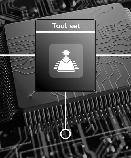
Tool set
J-Link PLUS comes with a versatile suite of software tools that enhance its performance and flexibility for debugging and programming. Utilities such as J-Link Commander, J-Link Configurator, and J-Link Remote Server make it a powerful and convenient tool for any development setup. Below are selected highlights from this tool set.

Embedded Studio
J-Link PLUS supports SEGGER Embedded Studio as well as virtually all Integrated Development Environments (IDEs), ensuring maximum flexibility in any development setup.
Ozone
It integrates seamlessly with SEGGER’s Ozone debugger, providing a powerful environment for performance analysis, instruction tracing, and code optimization.
J-Flash
J-Flash enables programming of microcontroller internal and external flash memories. Exceedingly versatile, it runs on Microsoft Windows, Linux, and macOS, and it supports Cortex Arm, RX, and RISC-V devices and cores.
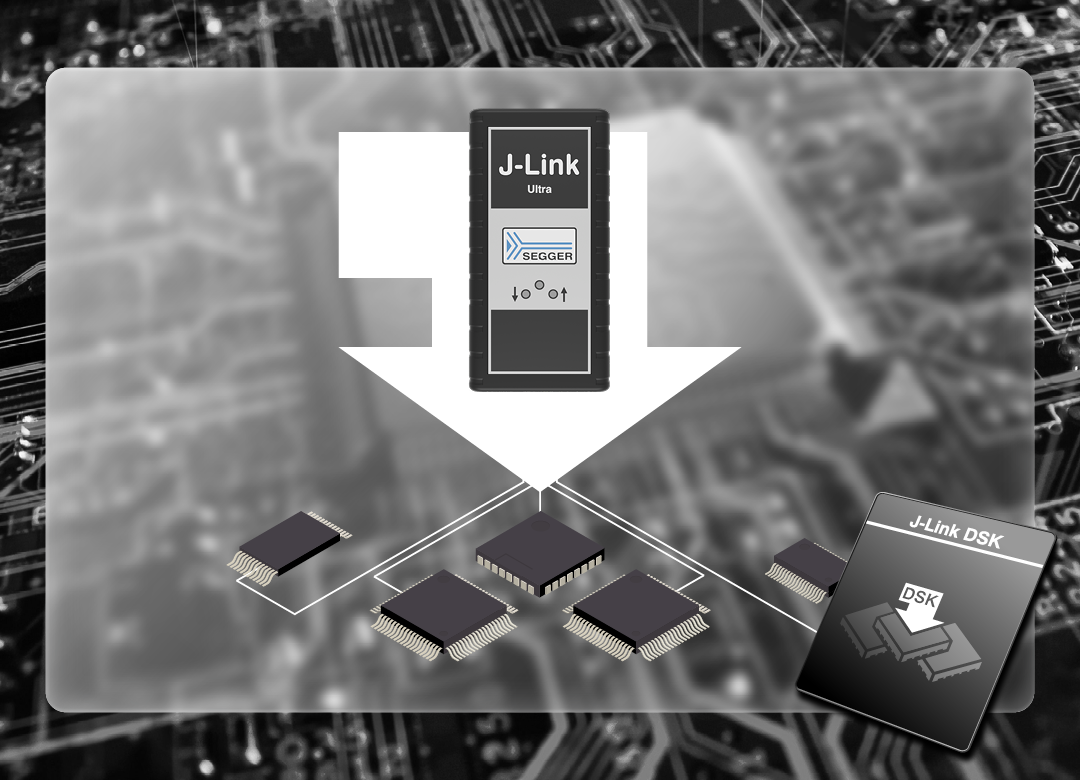
J-Link DSK
The J-Link Device Support Kit (DSK) allows silicon vendors and users to add debug and flash programming support for new devices. A new device typically requires a flash loader and, in some cases, a script defining special connect and reset sequences.
The DSK includes the SEGGER flash loader as well as a collection of example script files for devices that require special handling.
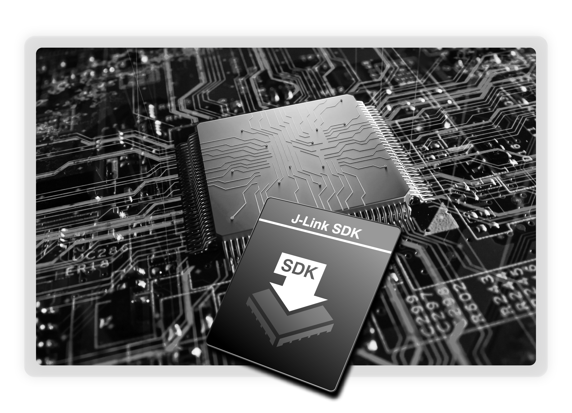
J-Link SDK
The J-Link Software Development Kit (SDK) enables the integration of J-Link and J-Trace support into custom applications. It is used in professional IDEs, such as SEGGER Embedded Studio, to enable direct debugging via J-Link / J-Trace, as well as in customized production utilities. Available for Windows, Linux, and macOS, the SDK can be used with nearly any programming language or solution.
Software
All software is included free of charge, as are licenses for all J-Link-related SEGGER software products, such as J-Link Unlimited Flash Breakpoints, Ozone, RDI, and J-Flash.
The J-Link Software and Documentation Package is available here:
Buyers Guide

J-Link BASE
Ethernet
J-Flash / J-Flash SPI
Unlimited Flash Breakpoints
Ozone
Monitor Mode
RDI
Real Time Transfer (RTT)
Download speed up to 1.0 MByte/sec
Target interface speed up to 15 MHz

J-Link PLUS
Ethernet
J-Flash / J-Flash SPI
Unlimited Flash Breakpoints
Ozone
Monitor Mode
RDI
Real Time Transfer (RTT)
Download speed up to 1.0 MByte/sec
Target interface speed up to 15 MHz

J-Link WiFi
Wireless Connection
J-Flash / J-Flash SPI
Unlimited Flash Breakpoints
Ozone
Monitor Mode
RDI
Real Time Transfer (RTT)
Download speed up to 1.0 MByte/sec
Target interface speed up to 15 MHz

J-Link Ultra
Ethernet
J-Flash / J-Flash SPI
Unlimited Flash Breakpoints
Ozone
Monitor Mode
RDI
Real Time Transfer (RTT)
Download speed up to 4.0 MByte/sec
Target interface speed up to 50 MHz

J-Link Pro
Ethernet
J-Flash / J-Flash SPI
Unlimited Flash Breakpoints
Ozone
Monitor Mode
RDI
Real Time Transfer (RTT)
Download speed up to 4.0 MByte/sec
Target interface speed up to 50 MHz

J-Link Pro PoE
Power over Ethernet
J-Flash / J-Flash SPI
Unlimited Flash Breakpoints
Ozone
Monitor Mode
RDI
Real Time Transfer (RTT)
Download speed up to 4.0 MByte/sec
Target interface speed up to 50 MHz
Customer support
J-Link PLUS comes with one year (12 months) of Basic Support. Beyond that, SEGGER's Extended Coverage gives users the option to extend the hardware warranty and Basic Support for one additional year (12 months) or two additional years (24 months). These options are only available at the time of purchase, either through the Web Shop or upon request; adding coverage at a later date is not possible.
Product images


Technical specifications
| General | |||||
|---|---|---|---|---|---|
| Supported OS | Microsoft Windows (x86/x64), Linux (x86/x64/Arm), macOS (x86/Apple Silicon) | ||||
| Electromagnetic compatibility (EMC) | EN 55022, EN 55024 | ||||
| Operating temperature | +5°C ... +60°C | ||||
| Storage temperature | -20°C ... +65 °C | ||||
| Relative humidity (non-condensing) | Max. 90% rH | ||||
| Mechanical | |||||
| Size of J-Link PLUS Classic (without cables) | 100mm x 53mm x 27mm | ||||
| Weight of J-Link PLUS Classic (without cables) | 70g | ||||
| Size of J-Link PLUS Compact (without cables) | 46mm x 46mm x 17mm | ||||
| Weight of J-Link PLUS Compact (without cables) | 20g | ||||
| Available Interfaces | |||||
| USB interface (J-Link PLUS Classic) | USB 2.0 (Hi-Speed); USB Type B | ||||
| USB interface (J-Link PLUS Compact) | USB 2.0 (Hi-Speed); USB-C | ||||
| Target interface | JTAG/SWD 20-pin (adapters available) | ||||
| JTAG/SWD Interface, Electrical | |||||
| Power supply | USB-powered Max. 50mA + Target Supply current. | ||||
| Target interface voltage (VIF) | 1.2V ... 5V | ||||
| Current drawn from target voltage sense pin (VTRef) | < 25µA | ||||
| Target supply voltage | 5V (derived from USB voltage) | ||||
| Target supply current | Max. 300mA | ||||
| Reset type | Open drain with 100 Ohms series resistor. Can be pulled low or tristated | ||||
| Reset low level output voltage (VOL) | VOL <= 10% of VIF | ||||
| For the whole target voltage range (1.2V <= VIF <= 5V) | |||||
| LOW level input voltage (VIL) | VIL <= 40% of VIF | ||||
| HIGH level input voltage (VIH) | VIH >= 60% of VIF | ||||
| For 1.2V >= VIF <= 3.6V | |||||
| LOW level output voltage (VOL) with a load of 10 kOhm | VOL <= 20% of VIF | ||||
| HIGH level output voltage (VOH) with a load of 10 kOhm | VOH >= 80% of VIF | ||||
| For 3.6 <= VIF <= 5V | |||||
| LOW level output voltage (VOL) with a load of 10 kOhm | VOL <= 20% of VIF | ||||
| HIGH level output voltage (VOH) with a load of 10 kOhm | VOH >= 80% of VIF | ||||
| JTAG/SWD Interface, Timing | |||||
| Target interface speed | Max. 15 MHz | ||||
| SWO sampling frequency | Max. 30 MHz | ||||
| Data input rise time (Trdi) | Tfdi <= 20ns | ||||
| Data output rise time (Trdo) | Trdo <= 10ns | ||||
| Data output fall time (Tfdo) | Tfdo <= 10ns | ||||
| Clock rise time (Trc) | Trc <= 3ns | ||||
| Clock fall time (Tfc) | Trc <= 3ns | ||||
FAQ
Can I use J-Flash with J-Link PLUS?
Yes. J-Link PLUS includes a preinstalled license for J-Flash on the probe itself. No setup is required — simply connect the J-Link PLUS and start using J-Flash.
What is the advantage of J-Link versus simple probes such as FTDI-based systems?
J-Link offers numerous advantages: the dedicated J-Link software provided by SEGGER, which enables seamless integration with common IDEs; the availability of Unlimited Flash Breakpoints for debugging software running in microcontroller flash memory; its high speed; and its simple, fast flash download capability.
In contrast to most simple probes, J-Link supports adaptive clocking as well as SWD and SWO. It also operates more reliably, as it is not merely a simple USB-to-JTAG converter. Instead, it uses the intelligence of its built-in CPU to ensure robust communication, particularly in situations where the target CPU runs at low clock speeds.
Can I work with more than one J-Link at the same time on the same machine?
Yes. You can connect any number of J-Links to your PC without additional configuration. Each J-Link is automatically registered with its unique serial number, allowing you to use multiple J-Links simultaneously.
I have multiple Arm cores in my JTAG chain. How can I debug them simultaneously with J-Link?
Two or more debuggers can use the same J-Link at the same time. Multi-core debugging requires multiple debuggers or multiple instances of the same debugger. Simply specify in your debugger which device in the scan chain you want to debug. No additional configuration is required.
Does J-Link support the Embedded Trace Buffer (ETB)?
Yes. J-Link supports ETB on Cortex-M3, Cortex-M4, Cortex-M7, and Cortex-A/R devices, if implemented by the target.
Does J-Link support the Micro Trace Buffer (MTB)?
Yes.
Does J-Link support the Embedded Trace Macrocell (ETM)?
No. ETM requires a separate connection to the Arm CPU and a device with built-in ETM support. ETM is supported by the J-Trace product family.
What is the maximum voltage that can be handled by the galvanic isolation of the Ethernet?
The Ethernet data lines are isolated in accordance with IEEE 802.3, with a test voltage of 1500 Vrms for one minute. This does not apply to the Ethernet shield, which has a direct electrical connection to the USB shield and resistive and capacitive coupling to the probe ground. For effective isolation, an unshielded twisted pair Ethernet cable must be used.
Latest news
Get in touch with us
Have questions or need assistance? Our Embedded Experts are here to help!
Reach out to us for:
- Licensing quotes
- Technical inquiries
- Project support